Schematic Diagram Samsung G318hz
[38+] dzkj schematic diagram tool download Bn44 smps syncmaster Motherboard pcb 4g mainboard circuit broadcom 3g
Samsung Galaxy S8 SM-G950D schematics
[download 36+] schematic diagram of android phone Schematic diagrams: bn44 00195 smps circuit diagram – for samsung Samsung s8 galaxy schematics sm
Schematic repairing schematics
Schematic tool diagram[get 19+] schematic diagram samsung g318hz T295 schematics mainboardSamsung schematic diagram free.
Plasma television us01 mortagne3/1/11 ~ mobile phone repair guides Samsung galaxy s8 sm-g950d schematicsSamsung galaxy tab a 8.0 sm-t295 schematics.

Samsung mengatasi
Wiring absCara mengatasi samsung g318hz lcd blank hitam [get 19+] schematic diagram samsung g318hzTv diagram lg samsung schematic led circuit lcd repair board schematics tips crt v3 interconnect wiring diagrams schema television collection.
.
![[Get 19+] Schematic Diagram Samsung G318hz](https://i2.wp.com/repairguide.autozone.com/znetrgs/repair_guide_content/en_us/images/0996b43f/80/25/52/64/large/0996b43f80255264.gif)

Samsung Galaxy Tab A 8.0 SM-T295 schematics
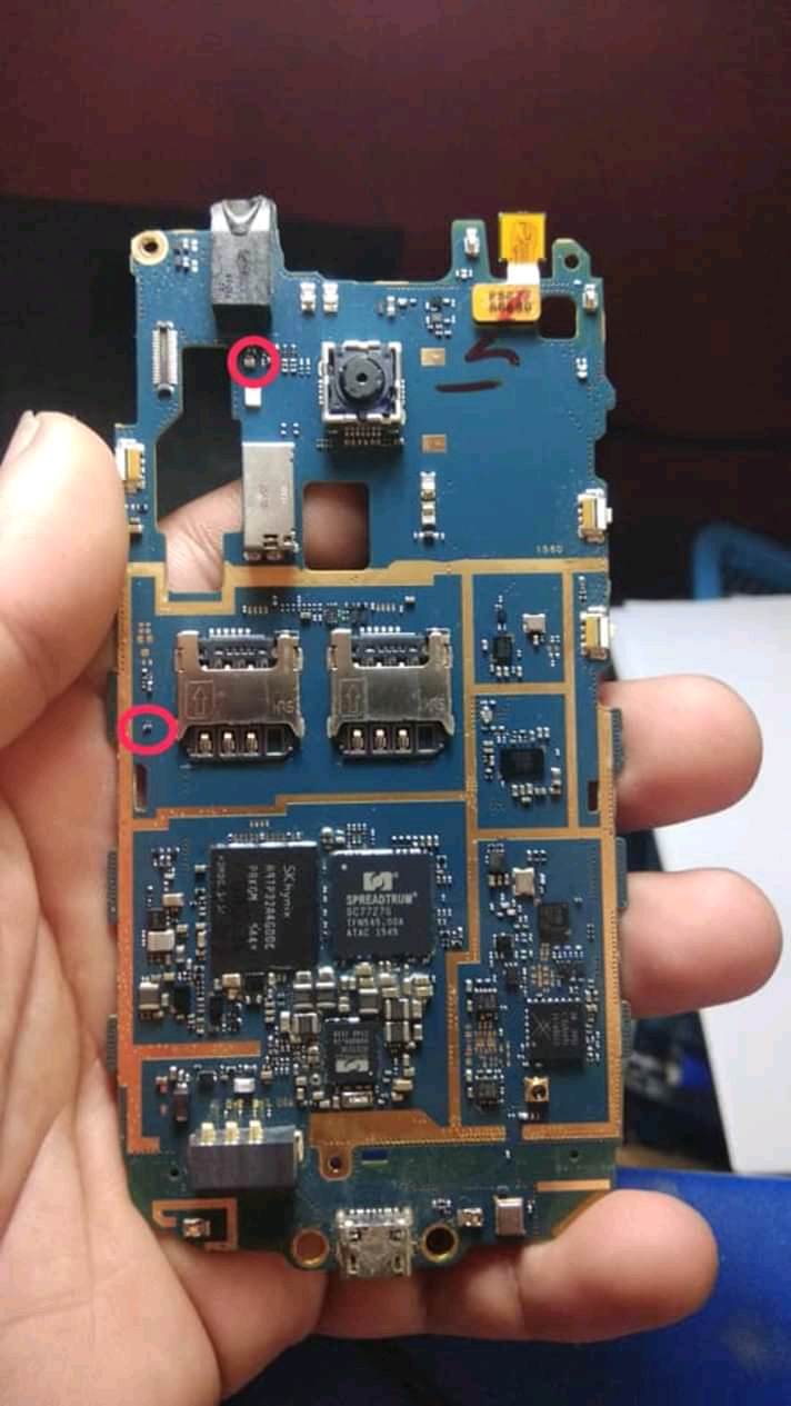
Cara Mengatasi Samsung G318HZ LCD Blank Hitam | service hp
![[Get 19+] Schematic Diagram Samsung G318hz](https://i2.wp.com/c.searspartsdirect.com/lis_png/PLDM/50042498-00001.png)
[Get 19+] Schematic Diagram Samsung G318hz

Samsung Galaxy S8 SM-G950D schematics

Schematic Diagrams: BN44 00195 SMPS circuit diagram – For Samsung
![[Download 36+] Schematic Diagram Of Android Phone](https://i.ytimg.com/vi/AlxXNjLFbhw/maxresdefault.jpg)
[Download 36+] Schematic Diagram Of Android Phone
![[38+] Dzkj Schematic Diagram Tool Download](https://1.bp.blogspot.com/-ba9d5tpuMkQ/WSopGurfNJI/AAAAAAAAAW4/j8VXSYga8Wseznl08jgCGpVVpTKFTCZKgCLcB/w1200-h630-p-k-no-nu/7b.JPG)
[38+] Dzkj Schematic Diagram Tool Download

Samsung Schematic Diagram Free - clipsprogs